Sunday, 23 February 2014

Temperature sensor (engineering project) digital thermometer


A digital thermometer can be made by interfacing a temperature sensor to a micro controller AT89C51, the temperature sensor used in this project is LM35. the variation in temperature is converted into to 10mV voltage signal that is received by analogue to digital convertor IC ADC0804 which convert it into 8-bit binary data, and serves as an input to the AT89C51. the LCD interfaced with other port of micro controller display the temperature in Fahrenheit.
project layout and the use of ic


LM35:

It is basically a transducer – a device used to convert some physical quantity in to some measurable electrical quantity for example current, voltage, capacitance or inductance depending on the circumstances. LM35 that is used in this project comes in an IC package. It has 3 pins. 2 are used for the power supply while the remaining one is used to pass on the voltage difference of 10mV produced by varying quantity. So its resolution is 10mV. The temperature in it directly proportional to change in temperature so any change in temperature is only detected if it hits the 10mV limit otherwise no change is experienced.

ADC0804:

 is a very commonly used 8-bit analog to digital convertor. It is a single channel IC, i.e., it can take only one analog signal as input. The digital outputs vary from 0 to a maximum of 255. The step size can be adjusted by setting the reference voltage at pin9. When this pin is not connected, the default reference voltage is the operating voltage, i.e., Vcc. The step size at 5V is 19.53mV (5V/255), i.e., for every 19.53mV rise in the analog input, the output varies by 1 unit. To set a particular voltage level as the reference value, this pin is connected to half the voltage. For example, to set a reference of 4V (Vref), pin9 is connected to 2V (Vref/2), thereby reducing the step size to 15.62mV (4V/255). ADC0804 needs a clock to operate. The time taken to convert the analog value to digital value is dependent on this clock source. An external clock can be given at the Clock IN pin. ADC 0804 also has an inbuilt clock which can be used in absence of external clock. A suitable RC circuit is connected between the Clock IN and Clock R pins to use the internal clock.

16x2 LCD Display:

CD (Liquid Crystal Display) screen is an electronic display module and find a wide range of applications. A 16x2 LCD display is very basic module and is very commonly used in various devices and circuits. These modules are preferred over seven segments and other multi segment LEDs. The reasons being: LCDs are economical; easily programmable; have no limitation of displaying special & even custom characters (unlike in seven segments), animations and so on.

A 16x2 LCD means it can display 16 characters per line and there are 2 such lines. In this LCD each character is displayed in 5x7 pixel matrix. This LCD has two registers, namely, Command and Data.
The command register stores the command instructions given to the LCD. A command is an instruction given to LCD to do a predefined task like initializing it, clearing its screen, setting the cursor position, controlling display etc. The data register stores the data to be displayed on the LCD. The data is the ASCII value of the character to be displayed on the LCD. Click to learn more about internal structure of a LCD.


Working: 

AT89C51 from the family of 8051 is used as a microcontroller in this embedded system application. Its port 1 is used an input port in order to fetch data from ADC0804. The received data is then converted into ASCII in order to be displayed at the 16x2 LCD which is interfaced at the port 2 of the AT89C51.

Links for detail 

digital thermometer
2  google images of digital thermometer
list of temperature sensor

Saturday, 22 February 2014

To measure phase voltages and currents in a three phase system(engineering students lab report)

Required Components:

AC voltage sources (Vac), resistors (R), voltmeters (Vprint2), ammeters (Iprint), ground (EGnd), and connecting wires.

Circuit Diagram

 this circuit diagram is drawn in pspice  software,you can download free software by clicking links below, to know more about pspice circuit software follow the links below


Procedure:

Open Schematics.
Go to get new parts, select and place the required parts. 
Place the components in their appropriate position and if necessary rotate by cntr+r.
Click on draw wire and connect all the elements.
Configure the values of all the placed elements.
Go to analysis, check AC sweep, open it, set total points to 1 and also set the frequency to 50 Hz.
Saves the circuit.
Go to analysis and simulate the circuit.
Go to analysis and examine the results.

Results

**** 01/01/12 20:02:09 *********** Evaluation PSpice (Nov 1999) **************
 * D:\pluto's projects\ckt lab rpt\11.sch
 ****     CIRCUIT DESCRIPTION
******************************************************************************
* Schematics Version 9.1 - Web Update 1
* Sun Jan 01 20:02:06 2012
** Analysis setup **
.ac LIN 1 50 50
.OP 
* From [PSPICE NETLIST] section of pspiceev.ini:
.lib "nom.lib"
.INC "11.net"
**** INCLUDING 11.net ****

* Schematics Netlist *


V_VAB         $N_0001 $N_0002 DC 0V AC 10V 0
V_PRINT2         $N_0003 $N_0004 0V

.PRINT        AC 
+ IM(V_PRINT2) 
+ IP(V_PRINT2)    
V_PRINT3         $N_0002 $N_0005 0V
          
.PRINT        AC 
+ IM(V_PRINT3) 
+ IP(V_PRINT3)    
           
.PRINT         AC 
+ VM([$N_0006],[0]) 
+ VP([$N_0006],[0])    
           
.PRINT         AC 
+ VM([$N_0004],[0]) 
+ VP([$N_0004],[0])    
R_RAB         $N_0001 $N_0007  1u  
R_RCA         $N_0008 $N_0007  1u  
R_RaN         0 $N_0006  1k  
R_RbN         $N_0005 0  1k  
R_RcN         $N_0004 0  1k  
           
.PRINT         AC 
+ VM([$N_0005],[0]) 
+ VP([$N_0005],[0])    
V_PRINT1         $N_0007 $N_0006 0V
          
.PRINT        AC 
+ IM(V_PRINT1) 
+ IP(V_PRINT1)    
R_RBC         $N_0002 $N_0009  1u  
V_VBC         $N_0009 $N_0003 DC 0V AC 10V -120
V_VCA         $N_0003 $N_0008 DC 0V AC 10V 120

**** 01/01/12 20:02:09 *********** Evaluation PSpice (Nov 1999) **************
 * D:\pluto's projects\ckt lab rpt\11.sch
 ****     SMALL SIGNAL BIAS SOLUTION       TEMPERATURE =   27.000 DEG C
******************************************************************************
 NODE   VOLTAGE     NODE   VOLTAGE     NODE   VOLTAGE     NODE   VOLTAGE
($N_0001)    0.0000                   ($N_0002)    0.0000                       

($N_0003)    0.0000                   ($N_0004)    0.0000                       

($N_0005)    0.0000                   ($N_0006)    0.0000                       

($N_0007)    0.0000                   ($N_0008)    0.0000                       

($N_0009)    0.0000                   

    VOLTAGE SOURCE CURRENTS
    NAME         CURRENT

    V_VAB        0.000E+00
    V_PRINT2     0.000E+00
    V_PRINT3     0.000E+00
    V_PRINT1     0.000E+00
    V_VBC        0.000E+00
    V_VCA        0.000E+00

    TOTAL POWER DISSIPATION   0.00E+00  WATTS

**** 01/01/12 20:02:09 *********** Evaluation PSpice (Nov 1999) **************
 * D:\pluto's projects\ckt lab rpt\11.sch
 ****     OPERATING POINT INFORMATION      TEMPERATURE =   27.000 DEG C
******************************************************************************

**** 01/01/12 20:02:09 *********** Evaluation PSpice (Nov 1999) **************
 * D:\pluto's projects\ckt lab rpt\11.sch

 ****     AC ANALYSIS                      TEMPERATURE =   27.000 DEG C
******************************************************************************

  FREQ        IM(V_PRINT2)IP(V_PRINT2)
   5.000E+01   5.774E-03   9.000E+01

**** 01/01/12 20:02:09 *********** Evaluation PSpice (Nov 1999) **************
 * D:\pluto's projects\ckt lab rpt\11.sch
 ****     AC ANALYSIS                      TEMPERATURE =   27.000 DEG C
******************************************************************************


  FREQ        IM(V_PRINT3)IP(V_PRINT3)
   5.000E+01   5.774E-03  -1.500E+02

**** 01/01/12 20:02:09 *********** Evaluation PSpice (Nov 1999) **************
 * D:\pluto's projects\ckt lab rpt\11.sch
 ****     AC ANALYSIS                      TEMPERATURE =   27.000 DEG C
******************************************************************************

  FREQ        VM($N_0006,0)VP($N_0006,0)
   5.000E+01   5.774E+00  -3.000E+01

**** 01/01/12 20:02:09 *********** Evaluation PSpice (Nov 1999) **************
 * D:\pluto's projects\ckt lab rpt\11.sch
 ****     AC ANALYSIS                      TEMPERATURE =   27.000 DEG C
******************************************************************************

  FREQ        VM($N_0004,0)VP($N_0004,0)
   5.000E+01   5.774E+00   9.000E+01

**** 01/01/12 20:02:09 *********** Evaluation PSpice (Nov 1999) **************
 * D:\pluto's projects\ckt lab rpt\11.sch
 ****     AC ANALYSIS                      TEMPERATURE =   27.000 DEG C
******************************************************************************

  FREQ        VM($N_0005,0)VP($N_0005,0)
   5.000E+01   5.774E+00  -1.500E+02

**** 01/01/12 20:02:09 *********** Evaluation PSpice (Nov 1999) **************
 * D:\pluto's projects\ckt lab rpt\11.sch
 ****     AC ANALYSIS                      TEMPERATURE =   27.000 DEG C
******************************************************************************

  FREQ        IM(V_PRINT1)IP(V_PRINT1)
   5.000E+01   5.774E-03  -3.000E+01
JOB CONCLUDED
TOTAL JOB TIME             .02


pspice free download links


To study the RLC ringing circuit

Required Components:

DC voltage Source (Vdc), Resistor (R), Capacitor (C), Inductor (L), normally closed switch (sw_topen), Ground (Gnd) and connecting wires.

Circuit Diagram

 this circuit diagram is drawn in pspice  software,you can download free software by clicking links below, to know more about pspice circuit software follow the links below


Procedure:

Open Schematics.
Go to get new parts, select and place the required components. 
Click on draw wire and connect all the elements.
Configure the values of all the placed elements.
Go to analysis   setup check transient.
Open transient  set print step and step ceiling to 1us, final time to 4ms and print delay to 0s.
Saves the circuit.
Don’t skip initial transient solution.
Go to analysis and simulate the circuit.
Go to OrCad window  Trace  Add Trace  I(C), V(C), I(L), V(L).
View the waveform.


Result


pspice free download links


To study the RLC transient circuit( engineering student lab report)

Required Components:

DC voltage Source (Vdc), Resistors (R), Capacitor (C), Inductor (L), normally closed switch (sw_topen), Ground (Gnd) and connecting wires.

Circuit Diagram

 this circuit diagram is drawn in pspice  software,you can download free software by clicking links below, to know more about pspice circuit software follow the links below


Procedure:

Open Schematics.
Go to get new parts, select and place the required components. 
Click on draw wire and connect all the elements.
Configure the values of all the placed elements.
Go to analysis   setup check transient.
Open transient  set print step and step ceiling to 1us, final time to 16ms and print delay to 0s.
Saves the circuit.
Don’t skip initial transient solution.
Go to analysis and simulate the circuit.
Go to OrCad window  Trace  Add Trace  I(C), V(C), I(L), V(L).
View the waveform.

Result


To study the RC transient circuit

Required Components:

DC voltage Source (Vdc), Resistor (R), Capacitor (C), normally open switch (sw_tclose), Ground (Gnd) and connecting wires.

Circuit Diagram

 his circuit diagram is drawn in pspice  software,you can download free software by clicking links below, to know more about pspice circuit software follow the links below

Procedure:

Open Schematics.
Go to get new parts, select and place the required components. 
Click on draw wire and connect all the elements.
Configure the values of all the placed elements.
Go to analysis   setup check transient.
Open transient  set print step and step ceiling to .5us, final time to 1ms and print delay to 0s.
Saves the circuit.
Go to analysis and simulate the circuit.
Go to OrCad window  Trace  Add Trace  I(C), V(C).
View the waveform.


Result


To study the RL transient circuit

Required Components:

DC voltage Source (Vdc), Resistor (R), Inductor (L), normally open switch (sw_tclose), Ground (Gnd) and connecting wires.

Circuit Diagram

this circuit diagram is drawn in pspice  software,you can download free software by clicking links below, to know more about pspice circuit software follow the links below


Procedure:

Open Schematics.
Go to get new parts, select and place the required components. 
Click on draw wire and connect all the elements.
Configure the values of all the placed elements.
Go to analysis   setup check transient.
Open transient  set print step and step ceiling to 10us, final time to 5ms and print delay to 0s.
Saves the circuit.
Go to analysis and simulate the circuit.
Go to OrCad window  Trace  Add Trace  I(L), V(L).
View the waveform.


Result

pspice free download links


To plot voltage, current and power waveform of an RLC circuit(engineering lab report)

Required Components:

Voltage Source (Vsin), Resistor (R), Inductor (L), Capacitor (C), Ground (Gnd) and connecting wires.

Circuit Diagram


Procedure:

Open Schematics.
Go to get new parts, select and place the required components. 
Click on draw wire and connect all the elements.
Configure the values of all the placed elements.
Go to analysis   setup check transient.
Open transient  set print step and step ceiling to 0.1ms, final time to 40ms and print delay to 0s.
Saves the circuit.
Go to analysis and simulate the circuit.
Go to OrCad window  Trace  Add Trace  I(R), V(R).
View the waveform.


Result


To plot voltage, current and power waveform of a resistive circuit

Required Components:
Voltage Source (Vsin), Resistor (R), Ground (Gnd) and connecting wires.

Required Components:

Voltage Source (Vsin), Resistor (R), Ground (Gnd) and connecting wires.

Circuit Diagram

this circuit diagram is drawn in pspice  software,you can download free software by clicking links below, to know more about pspice circuit software follow the links below
 

Procedure:

Open Schematics.
Go to get new parts, select a resister and an AC source (Vsin). 
Click on draw wire and connect all the elements.
Configure the values of all the placed elements.
Go to analysis   setup check transient.
Open transient  set print step and step ceiling to 0.2ms, final time to 60ms and print delay to 0s.
Saves the circuit.
Go to analysis and simulate the circuit.


Go to OrCad window  Trace  Add Trace  I(R), V(R).
View the waveform.

Result


To check the null (condition) of a bridge


Required Components:

Voltage Source (Vac), Resistors (R), Ammeters (Iprint), Ground (Gnd) and connecting wires.

Circuit Diagram

his circuit diagram is drawn in pspice  software,you can download free software by clicking links below, to know more about pspice circuit software follow the links below


Procedure:

Open Schematics.
Go to get new parts, select and place the required parts. 
Place the components in their appropriate position and if necessary rotate by cntr+r.
Click on draw wire and connect all the elements.
Configure the values of all the placed elements.
Go to analysis, check AC sweep, open it, set total points to 1 and also set the frequency to 50 Hz.
Saves the circuit.
Go to analysis and simulate the circuit.
Go to analysis and examine the results.

Results

**** 12/30/11 18:29:06 *********** Evaluation PSpice (Nov 1999) **************
 * D:\pluto's projects\ckt labs\4\dkt lab # 4.sch
 ****     CIRCUIT DESCRIPTION
******************************************************************************
* Schematics Version 9.1 - Web Update 1
* Fri Dec 30 18:27:43 2011
** Analysis setup **
.ac LIN 1 50 50
.OP 
* From [PSPICE NETLIST] section of pspiceev.ini:
.lib "nom.lib"
.INC "dkt lab # 4.net"
**** INCLUDING "dkt lab # 4.net" ****

* Schematics Netlist *

R_R2         $N_0002 $N_0001  10  
R_R4         $N_0004 $N_0003  100  
R_R3         $N_0001 $N_0003  100  
R_R6         $N_0002 0  2  
R_R5         0 $N_0003  20  
V_PRINT1         $N_0002 $N_0004 0V        
.PRINT        AC 
+ IM(V_PRINT1) 
+ IP(V_PRINT1)    
R_R1         $N_0005 $N_0001  1  
V_V1         $N_0005 0 DC 0V AC 10V 90
**** 12/30/11 18:29:06 *********** Evaluation PSpice (Nov 1999) **************
 * D:\pluto's projects\ckt labs\4\dkt lab # 4.sch
 ****     SMALL SIGNAL BIAS SOLUTION       TEMPERATURE =   27.000 DEG C
******************************************************************************
 NODE   VOLTAGE     NODE   VOLTAGE     NODE   VOLTAGE     NODE   VOLTAGE
($N_0001)    0.0000                   ($N_0002)    0.0000                       
($N_0003)    0.0000                   ($N_0004)    0.0000                       
($N_0005)    0.0000                   
    VOLTAGE SOURCE CURRENTS
    NAME         CURRENT
    V_PRINT1     0.000E+00
    V_V1         0.000E+00
    TOTAL POWER DISSIPATION   0.00E+00  WATTS

**** INCLUDING "dkt lab # 4.als" ****
* Schematics Aliases *


.ALIASES
R_R2            R2(1=$N_0002 2=$N_0001 )
R_R4            R4(1=$N_0004 2=$N_0003 )
R_R3            R3(1=$N_0001 2=$N_0003 )
R_R6            R6(1=$N_0002 2=0 )
R_R5            R5(1=0 2=$N_0003 )
V_PRINT1          PRINT1(1=$N_0002 2=$N_0004 )

R_R1            R1(1=$N_0005 2=$N_0001 )
V_V1            V1(+=$N_0005 -=0 )
.ENDALIASES**** 12/30/11 18:29:06 *********** Evaluation PSpice (Nov 1999) **************
 * D:\pluto's projects\ckt labs\4\dkt lab # 4.sch
 ****     OPERATING POINT INFORMATION      TEMPERATURE =   27.000 DEG C
*********************************************************************************
* 12/30/11 18:29:06 *********** Evaluation PSpice (Nov 1999) **************
 * D:\pluto's projects\ckt labs\4\dkt lab # 4.sch

 ****     AC ANALYSIS                      TEMPERATURE =   27.000 DEG C

******************************************************************************

  FREQ        IM(V_PRINT1)IP(V_PRINT1)

   5.000E+01   1.735E-18   9.000E+01
          JOB CONCLUDED
          TOTAL JOB TIME             .02
psice free download links 

To find various node voltages and voltage drops in a given circuit.


Required Components:

Voltage Sources (Vac), Resistors (R), Ammeters (Iprint), Voltmeters (Vprint1),  Inductor (L), Capacitor (C), Ground (Gnd) and connecting wires.


Circuit Diagram this circuit diagram is drawn in pspice  software,you can download free software by clicking links below, to know more about pspice circuit software follow the links below


Procedure:

Open Schematics.
Go to get new parts, select and place the required parts. 
Place the components in their appropriate position and if necessary rotate by cntr+r.
Click on draw wire and connect all the elements.
Configure the values of all the placed elements.
Go to analysis, check AC sweep, open it, set total points to 1 and also set the frequency to 50 Hz.
Saves the circuit.
Go to analysis and simulate the circuit.
Go to analysis and examine the results.

Results
**** 12/30/11 18:04:11 *********** Evaluation PSpice (Nov 1999) **************
 * D:\pluto's projects\ckt labs\3\ckt lab 3.sch

 ****     CIRCUIT DESCRIPTION

******************************************************************************
* Schematics Version 9.1 - Web Update 1
* Fri Dec 30 17:49:52 2011
** Analysis setup **
.ac LIN 1 50 50
.OP 
* From [PSPICE NETLIST] section of pspiceev.ini:
.lib "nom.lib"
.INC "ckt lab 3.net"
**** INCLUDING "ckt lab 3.net" ****

* Schematics Netlist *

R_R1         $N_0002 $N_0001  100  
R_R2         $N_0004 $N_0003  100        
V_PRINT1         $N_0005 $N_0002 0V          
V_PRINT2         $N_0003 $N_0006 0V        
V_PRINT5         $N_0001 $N_0004 0V          
V_PRINT6         $N_0001 $N_0007 0V          
V_PRINT7         $N_0003 $N_0008 0V         
R_R3         $N_0006 $N_0009  100  
V_V2         $N_0009 0 DC 0V AC 100V 
V_V1         $N_0005 0 DC 0V AC 100V 
L_L1         0 $N_0007  10mH  
C_C1         0 $N_0008  0.0001F  
****     AC ANALYSIS                      TEMPERATURE =   27.000 DEG C
******************************************************************************

  FREQ        VM($N_0003) 

   5.000E+01   5.017E+01
**** 12/30/11 18:04:11 *********** Evaluation PSpice (Nov 1999) **************
 * D:\pluto's projects\ckt labs\3\ckt lab 3.sch
 ****     AC ANALYSIS                      TEMPERATURE =   27.000 DEG C
******************************************************************************

  FREQ        VM($N_0001) 

   5.000E+01   4.707E+00
**** 12/30/11 18:04:11 *********** Evaluation PSpice (Nov 1999) **************
 * D:\pluto's projects\ckt labs\3\ckt lab 3.sch
 ****     AC ANALYSIS                      TEMPERATURE =   27.000 DEG C
******************************************************************************

  FREQ        IM(V_PRINT1)

   5.000E+01   9.989E-01
**** 12/30/11 18:04:11 *********** Evaluation PSpice (Nov 1999) **************
 * D:\pluto's projects\ckt labs\3\ckt lab 3.sch
 ****     AC ANALYSIS                      TEMPERATURE =   27.000 DEG C
******************************************************************************

  FREQ        IM(V_PRINT2)

   5.000E+01   4.994E-01
**** 12/30/11 18:04:11 *********** Evaluation PSpice (Nov 1999) **************
 * D:\pluto's projects\ckt labs\3\ckt lab 3.sch
 ****     AC ANALYSIS                      TEMPERATURE =   27.000 DEG C
******************************************************************************

  FREQ        IM(V_PRINT5)

   5.000E+01   4.994E-01
**** 12/30/11 18:04:11 *********** Evaluation PSpice (Nov 1999) **************
 * D:\pluto's projects\ckt labs\3\ckt lab 3.sch
 ****     AC ANALYSIS                      TEMPERATURE =   27.000 DEG C
*****************************************************************************

  FREQ        IM(V_PRINT6)

   5.000E+01   1.498E+00**** 12/30/11 18:04:11 *********** Evaluation PSpice (Nov 1999) **************
 * D:\pluto's projects\ckt labs\3\ckt lab 3.sch
 ****     AC ANALYSIS                      TEMPERATURE =   27.000 DEG C
******************************************************************************

  FREQ        IM(V_PRINT7)

   5.000E+01   1.576E-15
          JOB CONCLUDED
          TOTAL JOB TIME            0.00

 p spice free download links

To find the loop and branch currents in the given circuit.(engineering task)


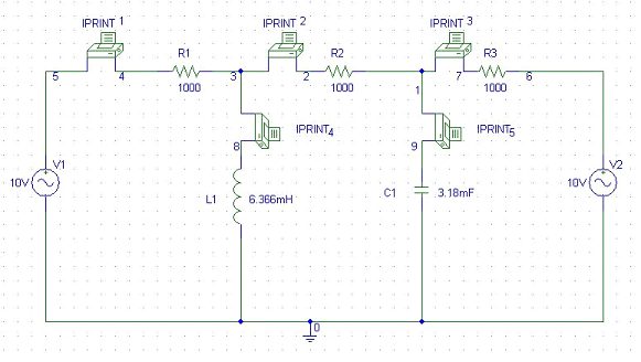
Required Components:

Voltage Sources (Vac), Resistors (R), Ammeters (Iprint), Inductor (L), Capacitor (C), Ground (Gnd) and connecting wires.


Circuit Diagram

this circuit diagram is drawn in pspice  software,you can download free software by clicking links below, to know more about pspice circuit software follow the links below


Procedure:

Open Schematics.
Go to get new parts, select and place the required parts.
Place the components in their appropriate position and if necessary rotate by cntr+r.
Click on draw wire and connect all the elements.
Configure the values of all the placed elements.
Go to analysis, check AC sweep, open it, set total points to 1 and also set the frequency to 50 Hz.
Saves the circuit.
Go to analysis and simulate the circuit.
Go to analysis and examine the results.

Result:

**** 12/30/11 16:53:55 *********** Evaluation PSpice (Nov 1999) **************
 * D:\pluto's projects\ckt labs\2\ckt lab 2.sch
****     CIRCUIT DESCRIPTION   ********
*********************************************************************
* Schematics Version 9.1 - Web Update 1
* Fri Dec 30 16:53:55 2011
** Analysis setup **
.ac LIN 1 50 50
.OP
* From [PSPICE NETLIST] section of pspiceev.ini:
.lib "nom.lib"
.INC "ckt lab 2.net"
**** INCLUDING "ckt lab 2.net" ****
* Schematics Netlist *
R_R2         $N_0002 $N_0001  1000
R_R1         $N_0004 $N_0003  1000
V_V1         $N_0005 0 DC 0V AC 10V
V_V2         $N_0006 0 DC 0V AC 10V
V_PRINT1         $N_0005 $N_0004 0V    
V_PRINT2         $N_0003 $N_0002 0V        
R_R3         $N_0007 $N_0006  1000
V_PRINT3         $N_0001 $N_0007 0V
L_L1         0 $N_0008  6.366mH
C_C1         0 $N_0009  3.18mF
V_PRINT4         $N_0003 $N_0008 0V        
V_PRINT5         $N_0001 $N_0009 0V        
**** 12/30/11 16:53:55 *********** Evaluation PSpice (Nov 1999) **************
* D:\pluto's projects\ckt labs\2\ckt lab 2.sch
 ****     OPERATING POINT INFORMATION      TEMPERATURE =   27.000 DEG C
******************************************************************************
**** 12/30/11 16:53:55 *********** Evaluation PSpice (Nov 1999) **************
 * D:\pluto's projects\ckt labs\2\ckt lab 2.sch
 ****     AC ANALYSIS                      TEMPERATURE =   27.000 DEG C
******************************************************************************
  FREQ        IM(V_PRINT1)
   5.000E+01   1.000E-02
**** 12/30/11 16:53:55 *********** Evaluation PSpice (Nov 1999) **************
 * D:\pluto's projects\ckt labs\2\ckt lab 2.sch
 ****     AC ANALYSIS                      TEMPERATURE =   27.000 DEG C
******************************************************************************
  FREQ        IM(V_PRINT2)
   5.000E+01   3.001E-05
**** 12/30/11 16:53:55 *********** Evaluation PSpice (Nov 1999) *************
 * D:\pluto's projects\ckt labs\2\ckt lab 2.sch
 ****     AC ANALYSIS                      TEMPERATURE =   27.000 DEG C
******************************************************************************
 FREQ        IM(V_PRINT3)
5.000E+01   1.000E-02
**** 12/30/11 16:53:55 *********** Evaluation PSpice (Nov 1999) **************
 * D:\pluto's projects\ckt labs\2\ckt lab 2.sch
 ****     AC ANALYSIS                      TEMPERATURE =   27.000 DEG C
******************************************************************************
  FREQ        IM(V_PRINT4)
   5.000E+01   1.000E-02
**** 12/30/11 16:53:55 *********** Evaluation PSpice (Nov 1999) **************
 * D:\pluto's projects\ckt labs\2\ckt lab 2.sch
 ****     AC ANALYSIS                      TEMPERATURE =   27.000 DEG C
******************************************************************************
  FREQ        IM(V_PRINT5)
   5.000E+01   1.000E-02
          JOB CONCLUDED
          TOTAL JOB TIME             .02

YOU might also like 

To find the current and voltage of unknown elements in the given circuit.(electrical engineering lab)

Required Components:

Voltage Source (Vac), Resistors (R), Ammeter (Iprint), Voltmeter (Vprint), Ground (Gnd) and connecting wires.


Circuit Diagram

this circuit diagram is drawn in pspice  software,you can download free software by clicking links below, to know more about pspice circuit software follow the links below

Procedure:

Open Schematics.
Go to get new parts, select and place the required parts. 
Place the components in their appropriate position and if necessary rotate by cntr+r.
Click on draw wire and connect all the elements.
Configure the values of all the placed elements.
Go to analysis, check AC sweep, open it, set total points to 1 and also set the frequency to 50 Hz.
Saves the circuit.
Go to analysis and simulate the circuit.
Go to analysis and examine the results.


Results:

**** 12/30/11 16:26:29 *********** Evaluation PSpice (Nov 1999) **************
 * D:\pluto's projects\ckt labs\1\ckt lab 1.sch
 ****     CIRCUIT DESCRIPTION    ******************
************************************************************
* Schematics Version 9.1 - Web Update 1
* Fri Dec 30 16:26:25 2011
** Analysis setup **
.ac LIN 1 50 50
.OP 
* From [PSPICE NETLIST] section of pspiceev.ini:
.lib "nom.lib"
.INC "ckt lab 1.net"
**** INCLUDING "ckt lab 1.net" ****
* Schematics Netlist *
V_PRINT1         $N_0001 $N_0002 0V    
.PRINT        AC       IM(V_PRINT1)
V_V1         $N_0001 0 DC 0V AC 10V 
R_R1         $N_0002 0  10             
.PLOT         AC       VM([$N_0002],[0])
* Schematics Aliases *
.ALIASES
V_PRINT1          PRINT1(1=$N_0001 2=$N_0002 )
V_V1            V1(+=$N_0001 -=0 )
R_R1            R1(1=$N_0002 2=0 )
.ENDALIASES
**** RESUMING "ckt lab 1.cir" ****
.probe
.END
**** 12/30/11 16:26:29 *********** Evaluation PSpice (Nov 1999) **************
 * D:\pluto's projects\ckt labs\1\ckt lab 1.sch
 ****     SMALL SIGNAL BIAS SOLUTION       TEMPERATURE =   27.000 DEG C
******************************************************************************
 NODE   VOLTAGE     NODE   VOLTAGE     NODE   VOLTAGE     NODE   VOLTAGE
($N_0001)    0.0000                   ($N_0002)    0.0000           
    VOLTAGE SOURCE CURRENTS
    NAME         CURRENT
    V_PRINT1     0.000E+00
    V_V1         0.000E+00
    TOTAL POWER DISSIPATION   0.00E+00  WATTS
**** 12/30/11 16:26:29 *********** Evaluation PSpice (Nov 1999) **************
 * D:\pluto's projects\ckt labs\1\ckt lab 1.sch
 ****     OPERATING POINT INFORMATION      TEMPERATURE =   27.000 DEG C
********************************************************************************** 12/30/11 16:26:29 *********** Evaluation PSpice (Nov 1999) **************
 * D:\pluto's projects\ckt labs\1\ckt lab 1.sch
 ****     AC ANALYSIS                      TEMPERATURE =   27.000 DEG C
******************************************************************************
  FREQ        IM(V_PRINT1)
   5.000E+01   1.000E+00**** 12/30/11 16:26:29 *********** Evaluation PSpice (Nov 1999) **************
 * D:\pluto's projects\ckt labs\1\ckt lab 1.sch
 ****     AC ANALYSIS                      TEMPERATURE =   27.000 DEG C
******************************************************************************
  FREQ        VM($N_0002,0)
(*)----------    1.0000E+01   1.0000E+02   1.0000E+03   1.0000E+04   1.0000E+05
                       _ _ _ _ _ _ _ _ _ _ _ _ _ _ _ _ _ _ _ _ _ _ _ _ _ _ _
  5.000E+01  1.000E+01 *            .            .            .            .
                       - - - - - - - - - - - - - - - - - - - - - - - - - - - 
          JOB CONCLUDED
          TOTAL JOB TIME             .02

YOU MAY ALSO LIKE


Friday, 14 February 2014

MOBILE ZONE: Smart bird (rebot)

MOBILE ZONE: Smart bird (rebot): links to image of smart bird smart bird is an automatic machine and is actually a reboot design to fly and in air and look like a natu...

here

Wednesday, 12 February 2014

To construct a Voltmeter and calibrating it, using potentiometer(engineering project)

Note: this is in image format, to view it better ,save the image and view it, its all about u. this project is perform by electrical engineering students of university of engineering and technology peshawar pakistan. one  of engineering can perform and practice it, this is simple an annul projects report and its main themes is given below.


Tuesday, 11 February 2014

Design and implement a Half Adder using NAND and NOT GATES

Half adder


Note: this is in image format, to view it better ,save the image and view it, its all about u. this project is perform by electrical engineering students of university of engineering and technology peshawar pakistan. one  of engineering can perform and practice it, this is simple an annul projects report and its main themes is given below

Design and implement a half subtracter using NAND and NOR Gates


Water level indicator( engineering project)


for further images click here google images
Note: this is in image format, to view it better ,save the image and view it, its all about u. this project is perform by electrical engineering students of university of engineering and technology peshawar pakistan. one  of engineering can perform and practice it, this is simple an annul projects report and its main themes is given below
refrences


Monday, 10 February 2014

Smart bird (rebot)

links to image of smart bird

smart bird is an automatic machine and is actually a reboot design to fly and in air and look like a natural bird name Herring_gull,
this smart bird is a new technology of Germany and used for various purposes , such is war and use in 2013 war in pakistan , afghanistan, india, and in iraq.
main feather of this bird is
its mas is 450 grams
its wingspan is 1.96 meter
look like Herring gull
can take off , fly and land by self
work on the principal of torsion mechanism and jet propulsion
made of Polyurethane_foam and Carbon_fiber
its brushless motor run at 23 watts
its wing push the air downward which is the action of smart bird and in the reaction air provide an upward force which keep the bird in air in this way it sustain in the air.
its is provided by two wheels attached to a rod which is connected with wings
direction is control by moving its tail just like a natural bird
it is made in GERMANY by a company name festo
Reference
animation
External links
youtube video
videos
its working,