Sunday 29 December 2013

C++ programming

this article is related with my previous topic , which was about c++ programming , here i m going to discuss that article more.

C++ programming

Std::cout

Standard output stream object
“Connected” to the screen
std:: specifies the "namespace" which cout belongs to
std:: can be removed by the use of using statements
with the help of using statement we can write cout instead of std::cout as we would observe in the next program.
<< 
Stream insertion operator 
Value to the right of the operator (right operand) inserted into output stream (which is connected to the screen)

std::cout << “Welcome to C++!\n”;


Indicates that a “special” character is to be output 


There are multiple ways to print text. Following are some more examples.

output 

Testing and debugging 

Bug
A mistake in a program
Debugging
Eliminating mistakes in programs
Term used when a moth caused a failed relay on the Harvard Mark 1 computer.  Grace Hopper and other programmers taped the moth in logbook stating:          “First actual case of a bug being found.”

Program errors

Syntax errors
Violation of the grammar rules of the language
Discovered by the compiler
Error messages may not always show correct location of errors
Run-time errors
Error conditions detected by the computer at run-time
Logic errors
Errors in the program’s algorithm
Most difficult to diagnose
Computer does not recognize an error

;;;;;;;;;;;;;;;;;;;;;;;;;;;;;;;;;;;;;;;;;;;;;;;;;;;;;;;;;;;;;;;;;;;;;;;;;;;;;;;;;;;;;;;;;;;;;;;;;;;;;;;;;;;;;;;;;;;;;;;;;;;;;;;;;;;;;;;;;;;;;;;;;;;;;;;;;;;;;;;;;

                                              murad ali shah .......... mobile zone;;;;;;;;;;;;;;we engineer the nation future 


computer programming in C++

in this article and in the incoming next articles i will cover all those topic , that will help you in writing a program , that is used in many designing eg in making calculator , logical operation etc , here its some describation of programming and a computer, or some mobile etc these programe are built in a device and come by default.

What is computer?

Computer
A device capable of performing computations and making logical decisions
A machine that manipulates data according to a list of instructions.
A programmable device that can store, retrieve, and process data.

Computer programs

Sets of instructions that control a computer’s processing of data

Hardware
Physical part of the computer
Various devices comprising a computer
Examples: keyboard, screen, mouse, disks, memory, CD-ROM, and processing units

Software
A collection of computer programs, procedures and documentation that perform some tasks on a computer system
Programs that run a computer

Computer organization

There are Six logical units in every computer:
Input unit
Obtains information (data and computer programs)  from input devices (keyboard, mouse)
Output unit
Outputs information to output device (screen, printer) or to control other devices.
Memory unit
 Rapid access, low capacity, stores input information
Arithmetic and logic unit (ALU)
Performs arithmetic calculations and logic decisions
Central processing unit (CPU)
Supervises and coordinates the other sections of the computer
Secondary storage unit
Cheap, long-term, high-capacity storage, stores inactive programs

Computer languages

Computer languages are divided into three types.
Machine languages
Machine language is machine dependent.
Strings of numbers giving machine specific instructions
Example:
+1300042774 +1400593419 +1200274027

Assembly languages

English-like abbreviations representing elementary computer operations (translated via assemblers)
Example:
  LOAD BASEPAY ADD OVERPAY STORE GROSSPAY
     Translator programs called assembler were developed to convert assembly language programs to machine language programs at computer speed.

High-level languages

Similar to everyday English, use mathematical notations (translated via compilers)
Example:
grossPay = basePay + overTimePay
C, C++ are the most widely used high level languages. Some other examples are
FORTRAN (formula translator)
         Used in scientific and engineering applications
COBOL (common business oriented language)
         Used to manipulate large amounts of data
Pascal
          Used to teach structured programming
Translator programs called Compilers converts high-level language programs into machine language

Object technology

Models the real world with groups of interacting objects

Object technology is a packaging scheme that helps create Meaningful software units
Date objects, time objects, paycheck objects, invoice objects, audio objects, video objects, file objects, record objects, etc.
Any noun can be represented as an object
Reusable software components that model real world items
More understandable, better organized and easier to maintain than procedural programming
Favor modularity
Java and C++ are popular object oriented languages.
Allows development of more error free and reliable software.

Basics of C++ environment 

Phases of C++ Programs    
       to be executed        
      1     EdiD
      2   process
      3    Compile
      4   Link
       5   Load
        6  Execute

Program organization

Program statement
Definition
Declaration
Action

Executable unit
Named set of program statements
Different languages refer to executable units by different names
Subroutine:  Fortran and Basic
Procedure: Pascal
Function : C++

C++ programming 

C++ program
Collection of  definitions, declarations and functions
Collection can span multiple files

Advantages
Structured into small understandable units
Complexity is reduced
Overall program size decreases
Pseudo code
Artificial, informal language used to develop algorithms
Similar to everyday English

Not executed on computers
Used to think out program before coding
Easy to convert into C++ program
Only executable statements
No need to declare variables
Algorithm
A sequence of precise instructions which leads to a solution
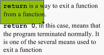
Program
An algorithm expressed in a language the computer can understand

program design 

Programming is a creative process

Program Design Process

Problem Solving Phase

Result is an algorithm that solves the problem

Implementation Phase
Result is the algorithm translated into a programming language
Program solving phase
Be certain the task is completely specified
What is the input?  
What information is in the output?  
How is the output organized?
Develop the algorithm before implementation
Experience shows this saves time in getting your program to run.
Test the algorithm for correctness

Implementation phase

Translate the algorithm into a programming language
Easier as you gain experience with the language
Compile the source code
Locates errors in using the programming language
Run the program on sample data
Verify correctness of results
Results may require modification of the algorithm and program
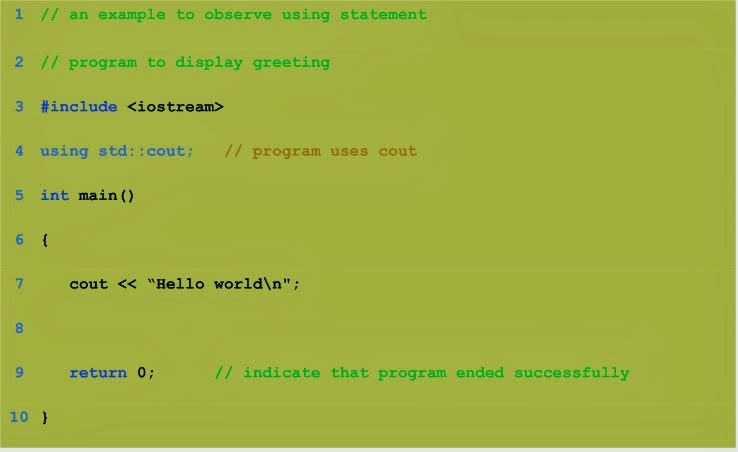


main program


comments


the part will be discuss in the next article


Sunday 15 December 2013

Bipolar Junction Transistors

my previous article was about programming and the uses of microprocessor in mobile phone , laptop and any device which is program , today i will talk about basic circuit elements and its uses in this post and in the next incoming post , from these circuit elements the basic circuit , a skeleton of a device is made, each elements has its own function , before learning modern techtenology it is neccessary to learn these basic ,electrical engineering is impossible without knowing these things, after my study i make a short form of it , which will be easy for the readers and will not consume his valuable time too much , lets have a look of it.

Introduction

A transistor is a device which can be used as either an amplifier or a switch. Let’s first consider it’s operation in a more simple view as a current controlling device
Basic Transistor Operation
Look at this one circuit as two separate circuits, the base-emitter(left side) circuit and the collector-emitter(right side) circuit. Note that the emitter leg serves as a conductor for both circuits.The amount of current flow in the base-emitter circuit controls the amount of current that flows in the collector circuit. Small changes in base-emitter current yields a large change in collector-current.
Transistor Structure
With diodes there is one p-n junction. With bipolar junction transistors (BJT), there are three three layers and two p-n junctions. Transistors can be a either pnp or npn type. 

Transistor Characteristics and Parameters

As previously discussed, base-emitter current changes yields large changes in collector-emitter current. The factor of this change is called beta
beta = IC/IB
There are three key dc voltages and three key dc currents to be considered. Note that these measurements are important for troubleshooting. 
IB: dc base current 
IE: dc emitter current
IC: dc collector current
VBE: dc voltage across base-emitter junction
VCB: dc voltage across collector-base junction
VCE: dc voltage from collector to emitter
For proper operation the base-emitter junction is forward biased by VBB and conducts just like a diode. 
The collector-base junction is reverse biased by VCC and blocks current flow through it’s junction just like a diode.
Remember current flow through the base-emitter junction will help establish the path for current flow from the collector to emitter. 
Analysis of this transistor circuit to predict the dc voltages and currents requires use of Ohm’s law, Kirchhoff’s voltage law and the beta for the transistor. 
Application of these laws begins with the base circuit to determine the amount of base current. Using Kichhoff’s voltage law, subtract the .7 VBE and the remaining voltage is dropped across RB. Determining the current for the base with this information is a mThe collector current is determined by multiplying the base current by beta. atter of applying of Ohm’s law.  VRB/RB = IB

What we ultimately determine by use of Kirchhoff’s voltage law for series circuits is that in the base circuit VBB is distributed across the base-emitter junction and RB in the base circuit. In the collector circuit we determine that VCC is distributed proportionally across RC and the transistor(VCE)
Collector characteristic curves gives a graphical illustration of the relationship of collector current and VCE with specified amounts of base current. With greater increases of VCC , VCE continues to increase until it reaches breakdown, but the current remains about the same in the linear region from .7V to the breakdown voltage.
With no IB the transistor is in the cutoff region and just as the name implies there is practically no current flow in the collector part of the circuit. With the transistor in a cutoff state the the full VCC can be measured across the collector and emitter(VCE)
Current flow in the collector part of the circuit is, as stated previously, determined by IB multiplied by . However, there is a limit to how much current can flow in the collector circuit regardless of additional increases inOnce this maximum is reached, the transistor is said to be in saturation. Note that saturation can be determined by application of Ohm’s law. IC(sat)=VCC/RC The measured voltage across this now seemingly “shorted” collector and emitter is 0V. IB. 
The dc load line graphically illustrates IC(sat) and Cutoff for a transistor
The beta for a transistor is not always constant. Temperature and collector current both affect beta, not to mention the normal inconsistencies during the manufacture of the transistor.
There are also maximum power ratings to consider. 
The data sheet provides information on these characteristics..
in the next article i will let u know about transistor amplifier and transistor switch . be in tough with this blog and learn more and more..................continue


iphone

a new look , its cool


Memory Map and Addresses of microprocessor

The memory map is a picture representation of the address range and shows where the different memory chips are located within the address range.

Address Range of a Memory Chip

The address range of a particular chip is the list of all addresses that are mapped to the chip.

An example for the address range and its relationship to the memory chips would be the Post Office Boxes in the post office.
Each box has its unique number that is assigned sequentially. (memory locations)
The boxes are grouped into groups. (memory chips)
The first box in a group has the number immediately after the last box in the previous group.

Address Range of a Memory Chip

The above example can be modified slightly to make it closer to our discussion on memory.
Let’s say that this post office has only 1000 boxes. 
Let’s also say that these are grouped into 10 groups of 100 boxes each. Boxes 0000 to 0099 are in group 0, boxes 0100 to 0199 are in group 1 and so on.

We can look at the box number as if it is made up of two pieces:
The group number and the box’s index within the group. 
So, box number 436 is the 36th box in the 4th group.

The upper digit of the box number identifies the group and the lower two digits identify the box within the group.

The 8085 and Address Ranges

The 8085 has 16 address lines. So, it can address a total of 64K memory locations.
If we use memory chips with 1K locations each, then we will need 64 such chips. 
The 1K memory chip needs 10 address lines to uniquely identify the 1K locations.  (log21024 = 10)
That leaves 6 address lines which is the exact number needed for selecting between the 64 different chips (log264 = 6).

The 8085 and Address Ranges

Now, we can break up the 16-bit address of the 8085 into two pieces:

A15 A14 A13 A12 A11 A10  A9 A8 A7 A6 A5 A4 A3 A2 A1 A0 


Depending on the combination on the address lines A15 - A10 , the address range of the specified chip is determined.

Chip Select Example

A chip that uses the combination A15  - A10 = 001000 would have addresses that range from 2000H to 23FFH.
Keep in mind that the 10 address lines on the chip gives a range of 00 0000 0000 to 11 1111 1111 or 000H to 3FFH for each of the chips.
The memory chip in this example would require the following circuit on  its chip select input:
To illustrate this with a picture:
in the first case, the memory chip occupies the piece of the memory map identified as before. 
In the second case, it occupies the piece identified as after.

High-Order vs. Low-Order Address Lines

The address lines from a microprocessor can be classified into two types:
High-Order
Used for memory chip selection
Low-Order
Used for location selection within a memory chip.

This classification is highly dependent on the memory system design.

Data Lines

All of the above discussion has been regarding memory length. Lets look at memory width. 
We said that the width is the number of bits in each memory word. 
We have been assuming so far that our memory chips have the right width. 
What if they don’t?
It is very common to find memory chips that have only 4 bits per location. How would you design a byte wide memory system using these chips?
We use two chips for the same address range. One chip will supply 4 of the data bits per address and the other chip supply the other 4 data bits for the same address.

Data Lines


Saturday 14 December 2013

Microprocessor Architecture used in mobile phone

in this article and in the next article  you will learn about memory and addresses of a memory location , in which information, data, are store 

The Design of a Memory Chip

Using the RD and WR controls we can determine the direction of flow either into or out of memory. Then using the appropriate Enable input we enable an individual memory register.

What we have just designed is a memory with 4 locations and each location has 4 elements (bits). This memory would be called 4 X 4 [Number of location X number of bits per location].

The Enable Inputs

How do we produce these enable line?
Since we can never have more than one of these enables active at the same time, we can have them encoded to reduce the number of lines coming into the chip.
These encoded lines are the address lines for memory. 

The Design of a Memory Chip

So, the previous diagram would now look like the following:

The Design of a Memory Chip

Since we have tri-state buffers on both the inputs and outputs of the flip flops, we can actually use one set of pins only.
The chip would now look like this:

the steps of writing into Memory

What happens when the programmer issues the STA instruction?
The microprocessor would turn on the WR control (WR = 0) and turn off the RD control (RD = 1).
The address is applied to the address decoder which generates a single Enable signal to turn on only one of the memory registers.
The data is then applied on the data lines and it is stored into the enabled register.

Dimensions of Memory

Memory is usually measured by two numbers: its length and its width (Length X Width).
The length is the total number of locations.
The width is the number of bits in each location.

The length (total number of locations) is a function of the number of address lines.
# of memory locations = 2( # of address lines)

So, a memory chip with 10 address lines would have 
210 = 1024 locations (1K)

Looking at it from the other side, a memory chip with 4K locations would need 
Log2 4096=12 address lines

The 8085 and Memory

The 8085 has 16 address lines. That means it can address 
216 = 64K memory locations. 
Then it will need 1 memory chip with 64 k locations, or 2 chips with 32 K in each, or 4 with 16 K each or 16 of the 4 K chips, etc.

how would we use these address lines to control the multiple chips?

Chip Select

Usually, each memory chip has a CS (Chip Select) input. The chip will only work if an active signal is applied on that input.

To allow the use of multiple chips in the make up of memory, we need to use a number of the address lines for the purpose of “chip selection”.
These address lines are decoded to generate the 2n necessary CS inputs for the memory chips to be used.

Chip Selection Example

Assume that we need to build a memory system made up of 4 of the 4 X 4 memory chips we designed earlier.

We will need to use 2 inputs and a decoder to identify which chip will be used at what time. 

The resulting design would now look like the one on the following slide.

Chip Selection Example


for further detail and any query you can mail on muradalishah57@yahoo.com or can call on +923329473428, 
https://www.google.com.pk/url?sa=t&rct=j&q=&esrc=s&source=web&cd=1&cad=rja&ved=0CCwQFjAA&url=http%3A%2F%2Fen.wikipedia.org%2Fwiki%2FMicroprocessor&ei=ZXWtUveFJozN7Abq3YHQDw&usg=AFQjCNELdGXZS5JPzHDs9j6hJNdWlSLE-A&sig2=Q81X9sIqEa1ta5p6Tc37CA&bvm=bv.57967247,d.ZGU

Microprocessor Architecture(mobile)

as i discuss in the previous post about memory element and various topic that are releated to microprocessor architecture that is use in htc ,android and and many cell phones leptops etc microprocessor is the main part of any operating system and other words it is the control, basic of a mobile , 

The Basic Memory Element

The basic memory element is similar to a D latch.
This latch has an input where the data comes in. It has an enable input and an output on which data comes out.

The Basic Memory Element

However, this is not safe.
Data is always present on the input and the output is always set to the contents of the latch.
To avoid this, tri-state buffers are added at the input and output of the latch.

The Basic Memory Element

The WR signal controls the input buffer.
The bar over WR means that this is an active low signal.
So, if WR is 0 the input data reaches the latch input.
If WR is 1 the input of the latch looks like a wire connected to nothing.
The RD signal controls the output in a similar manner.

A Memory “Register”

If we take four of these latches and connect them together, we would have a 4-bit memory register

A group of memory registers

Expanding on this scheme to add more memory registers we get the diagram to the right.

A group of Memory Registers

If we represent each memory location (Register) as a block we get the following


Microprocessor elements

We have already discussed the general purpose registers, the Accumulator, and the flags.

The Internal Architectureo

The Program Counter (PC)
This is a register that is used to control the sequencing of the execution of instructions.
This register always holds the address of the next instruction.
Since it holds an address, it must be 16 bits wide.
The Stack pointer
The stack pointer is also a 16-bit register that is used to point into memory. 
The memory this register points to is a special area called the stack.
The stack is an area of memory used to hold data that will be retreived soon.
The stack is usually accessed in a Last In First Out (LIFO) fashion.

Externally Initiated Operations

External devices can initiate (start) one of the 4 following operations:
Reset 
All operations are stopped and the program counter is reset to 0000.
Interrupt
The microprocessor’s operations are interrupted and the microprocessor executes what is called a “service routine”.
This routine “handles” the interrupt, (perform the necessary operations). Then the microprocessor returns to its previous operations and continues.
Ready
The 8085 has a pin called RDY. This pin is used by external devices to stop the 8085 until they catch up.
As long as the RDY pin is low, the 8085 will be in a wait state.
Hold
The 8085 has a pin called HOLD. This pin is used by external devices to gain control of the busses.
When the HOLD signal is activated by an external device, the 8085 stops executing instructions and stops using the busses.
This would allow external devices to control the information on the busses. Example DMA.

The Design and Operation of Memory

Memory in a microprocessor system is where information (data and instructions) is kept. It can be classified into two main types:
Main memory (RAM and ROM) 
Storage memory (Disks , CD ROMs, etc.)

The simple view of RAM is that it is made up of registers that are made up of flip-flops (or memory elements). 
The number of flip-flops in a “memory register” determines the size of the memory word.
ROM on the other hand uses diodes instead of the flip-flops to permanently hold the information.

Accessing Information in Memory


For the microprocessor to access (Read or Write) information in memory (RAM or ROM), it needs to do the following:
Select the right memory chip (using part of the address bus).
Identify the memory location (using the rest of the address bus).
Access the data (using the data bus).

Tri-State Buffers

An important circuit element that is used extensively in memory.
This buffer is a logic circuit that has three states:
Logic 0, logic1, and high impedance.
When this circuit is in high impedance mode it looks as if it is disconnected from the output completely.


The Tri-State Buffer

This circuit has two inputs and one output.
The first input behaves like the normal input for the circuit.
The second input is an “enable”.
If it is set high, the output follows the proper circuit behavior.
If it is set low, the output looks like a wire connected to nothing.

The Basic Memory Element

The basic memory element is similar to a D latch.
This latch has an input where the data comes in. It has an enable input and an output on which data comes out.
                                     

the remaining part of the topic will be post in the new article very soon , be in tough with this blog to read more .............


Microprocessor Architecture(used in mobile )

In this post i will cover all those internal architecture of an microprocessor that is the building block of all mobiles, egg htc , android etc anyone can study it in short but explanatory form , not only mobiles, but also computers, leptopes having this basic, which is describe below, in this post i discussed a lilttle about microprocessor but will cover and explain all knowledge about this in different post.
The microprocessor can be programmed to perform functions on given data by writing specific instructions into its memory.
The microprocessor reads one instruction at a time, matches it with its instruction set, and performs the data manipulation specified.
The result is either stored back into memory or displayed on an output device.

The 8085 Architecture

The 8085 uses three separate busses to perform its operations
The address bus.
The data bus.
The control bus.
16 bits wide (A0 A1…A15)
Therefore, the 8085 can access locations with numbers from 0 to 65,536. Or, the 8085 can access a total of 64K addresses.

“Unidirectional”.
Information flows out of the microprocessor and into the memory or peripherals.

When the 8085 wants to access a peripheral or a memory location, it places the 16-bit address on the address bus and then sends the appropriate control signals
Data bus
8 bits wide (D0 D1…D7)
“Bi-directional”.
Information flows both ways between the microprocessor and memory or I/O.

The 8085 uses the data bus to transfer the binary information.

Since the data bus has 8-bits only, then the 8085 can manipulate data 8 bits at-a-time only
Control bus
There is no real control bus. Instead, the control bus is made up of a number of single bit control signals
operation type in microprocessor
All of the operations of the microprocessor can be classified into one of three types:
Microprocessor Initiated Operations
Internal Operations
Peripheral Initiated Operations
Microprocessor initiated operation
These are operations that the microprocessor itself starts.
These are usually one of 4 operations:
Memory Read
Memory Write
I/O Read (Get data from an input device)
I/O write (Send data to an output device)
It is important to note that the microprocessor treats memory and I/O devices the same way.
Input and output devices simply look like memory locations to the microprocessor.
For example, the keyboard may look like memory address A3F2H. To get what key is being pressed, the microprocessor simply reads the data at location A3F2H.

The communication process between the microprocessor and peripheral devices consist of the following three steps:
Identify the address.
Transfer the binary information.
Provide the right timing signals.
Red operation
To read the contents of a memory location, the following steps take place:
The microprocessor places the 16-bit address of the memory location on the address bus.
The microprocessor activates a control signal called “memory read” which enables the memory chip.
The memory decodes the address and identifies the right location.
The memory places the contents on the data bus.
The microprocessor reads the value of the data bus after a certain amount of time.
internal data operation
The 8085 can perform a number of internal operations. Such as: storing data, Arithmetic & Logic operations, Testing for condition, etc.
To perform these operations, the microprocessor needs an internal architecture similar to the following: